Customer makes industry-leading semiconductor IP that advance data center connectivity and solve the bottleneck between memory and processing.
Design Team started supporting on High-speed PCB design in 2012 for their new India design centre.
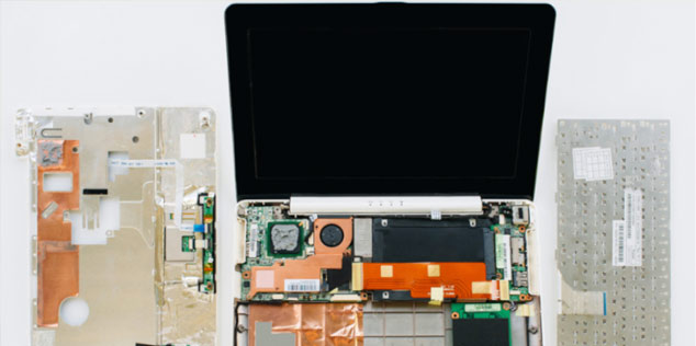
As per ECAD ‘first time right design’ approach, the customer’s U.S.A HQ did the PCB assembly in U.S and the design was proven to perform well.
Customer moved to next stage of PCB assembly to build their PCB Assembly with Avalon, Bangalore in 2013.
The first PCBA needed an expensive custom tool to mount a press fit connector on the PCB. Avalon with its vast experience on tooling and jigs, built this tool inhouse saving thousands of dollars to Customer and establishing Avalon as a long term supplier.
Today Avalon team have been exclusively building designs and PCBA’s and shipping to various locations of in Japan, Europe and U.S.
These are technologically advance PCBAs for advanced memory technology IP including DDR6 reference boards.
Design Team would have done more than 100 designs for Customer. More than 50 types would have been assembled directly for customer verification testing.
Remaining designs done by Design Team were shipped by customer as IP to world’s leading memory chip makers.
Customer has grown their design centre operations and is one of the largest design centre outside of their U.S office.
- Layers : 14 Layers Special Technology : Back drills 12 – 4 .
- Components on Board : 1500 + Components (Including discrete) : 70+ Packages.
- BGA Components : 5 high pincount BGA’s
- Material : Megtron 6
- Workflow – PCB Design, PCB Assembly in NPI