pcb-design
Avalontec's expertise in PCB design and electronic manufacturing services.
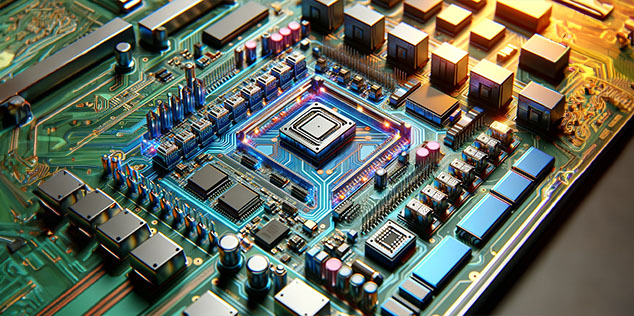
Revolutionizing PCB Design The SIENNA ECAD Edge in Electronic Design Automation
In the rapidly evolving world of electronic design, the complexity and requirements of printed circuit board (PCB) designs are at an all-time high. At SIENNA ECAD, we’re at the forefront of this revolution, leveraging cutting-edge technology and expert insight to drive innovation in PCB design and analysis. This blog explores how our expertise in complex layouts, SI/PI analysis, and more is shaping the future of Electronic Design Automation (EDA).
The Evolution of PCB Design
PCB design has come a long way from simple single layouts to highly complex, multi-layered designs. Through hole technology to laser drill technology. Rigid boards to flex boards. Components on outer layer to components inside the board. Frequency of KHz to GHz. With electronic devices becoming smaller yet more powerful, the demand for sophisticated PCB designs is more critical than ever. Here at SIENNA ECAD, our 26 years of journey has been marked by constant innovation and adaptation to these ever-changing needs.
Our Comprehensive Services
Complex Layouts
Our team excels in creating intricate designs that meet the specific needs of modern electronics, ensuring optimal performance and reliability.
SI, PI, Thermal & EMI Analysis
We use advanced techniques to analyze signal integrity, power integrity, thermal integrity, and electromagnetic interference, ensuring your PCBs are electrically not just well-designed but also robust and efficient.
Reliability and DFX
Our focus on design for excellence (DFX- DFA,DFF,DFT) ensures that each PCB is not only reliable, durable, cost-effective also ensures shorter duration & time to market.
Case Study Overcoming Design Challenges in the IoT Space
We recently partnered with a leading IoT company to address a unique design challenge. The client required a PCB design that could withstand extreme environmental conditions while maintaining high-speed performance. Our team’s expertise in thermal analysis and material selection led to a design that not only met but exceeded the client’s expectations.
The SIENNA ECAD Difference
State-of-the-Art Tools We employ the latest CAE software tools to offer innovative solutions in the EDA field.
Global Expertise, Local Solutions: With facilities in the USA and India, we bring global insights to local challenges, providing tailored solutions to our diverse client base.
Market Segment Focus: Our expertise spans various segments like Networking, Power, Transportation, Semiconductor, IoT, and Medical, enabling us to deliver specialized solutions across industries.
Looking Ahead The Future of PCB Design with SIENNA ECAD
As we look to the future, our commitment to excellence and innovation remains steadfast. With the electronic landscape continuously evolving, SIENNA ECAD is poised to not just keep up but lead the way in PCB design and analysis.
SIENNA ECAD is more than just a PCB design company; we are a hub of innovation and excellence. Whether you’re looking for complex PCB layouts or comprehensive analysis, our team is ready to deliver solutions that drive your electronic products to the next level.
FAQs About Contract Manufacturing
What is PCB design and why is it essential for U.S. electronics development?
PCB design lays out the electrical blueprint of your product. In the U.S., effective PCB design ensures signal integrity, manufacturability, and reliability—key to avoiding costly redesigns and launch delays.
What EMS services are typically bundled with PCB design for U.S. projects?
U.S. companies often combine PCB design with prototyping, PCB assembly (SMT/through-hole), box-build integration, cable harness fabrication, and testing—creating a seamless path from concept to production.
How do design-led EMS providers accelerate product readiness in the U.S.?
By bridging design and manufacturing under one roof, they reduce handoff issues, enable quicker iteration, ensure quality consistency, and cut lead times—supporting faster market entry for U.S. clients.
Can design-focused EMS firms accommodate iterative development needs?
Yes. They offer agile workflows—allowing revisions mid-cycle, rapid prototyping, and smooth scaling—all without disrupting the overall production timeline, catering to U.S. product development needs.
What are the top advantages of integrating PCB design and EMS under one provider in the U.S.?
Top benefits include unified design-manufacture coordination, fewer failure points, improved production reliability, streamlined testing, and hassle-free compliance—a stronger solution for U.S. product launches.
How does Avalon Technologies support U.S. customers with PCB design and full EMS services?
Avalon Technologies offers end-to-end solutions—from PCB layout and DFM review to assembly and system integration—through its U.S. and India sites. That means U.S. customers get design-grade support, manufacturing excellence, and managed deliveries without needing local production infrastructure.
At Avalon Technologies, we firmly believe that contract manufacturing excellence is the key to unlocking your business’s potential. By partnering with specialized manufacturers and embracing outsourcing, OEM manufacturers can focus on their core competencies. Contract manufacturing allows us to stay agile, adaptable, and efficient in a rapidly evolving market. Explore the possibilities of contract manufacturing and take your business to new heights with Avalon Technologies.